As automotive electronic systems continue to advance toward higher data rates, greater intelligence, and increased connectivity, the volume ofin-vehicle data transmission is also growing rapidly. High-frequency and high-speed interconnects—including FAKRA, Mini FAKRA, HSD, and Automotive Ethernet connectors—have therefore become essential elements of in-vehicle communication architectures.
Determining whether a high-frequency connector meets its design requirements cannot rely solely on appearance, dimensional inspection, or conventional electrical tests. A properly designed PCB test fixture is also essential for validating key electrical parameters such as impedance, insertion loss, return loss, and crosstalk.
In high-frequency testing, the fixture is not merely a mechanical means of holding the device under test (DUT); it is part of the overall signal path. The PCB stackup, routing, grounding, launch transitions, and impedance control of the fixture can all directly affect the measurement results. If the fixture is not properly designed, reflections, loss, or interference introduced by the fixture may distort the measured data—even when the DUT itself performs as intended.
.png)
HULANE has established a comprehensive high-frequency product validation process that integrates test fixture design, signal integrity analysis, electromagnetic simulation, measurement validation, and de-embedding. By minimizing fixture-induced effects, this process more accurately characterizes the intrinsic electrical performance of the product and provides reliable data for design optimization and product validation.
Why Do High-Frequency Test Fixtures Affect Measurement Results?
At GHz frequencies, measured data does not represent the DUT alone. It reflects the combined effects of the DUT, test fixtures, launch transitions, cables, adapters, and measurement equipment.
Any impedance discontinuity, excessive trace length, inadequate grounding, or structural asymmetry in the signal path can introduce signal reflections, transmission loss, crosstalk, and mode conversion. These effects can influence measured insertion loss, return loss, and impedance.
The primary objective of a high-frequency test fixture is therefore to be as electrically transparent as possible. In other words, the fixture should add minimal electrical influence so that the measured results represent the intrinsic characteristics of the DUT rather than the combined response of the DUT and fixture.
Achieving this objective requires careful control of impedance continuity, transmission loss, differential symmetry, signal return paths, and grounding structures.
Three Core Considerations in High-Frequency Test Fixture Design
1. Maintain Impedance Continuity to Minimize Reflections
Impedance control is one of the fundamental requirements of high-frequency fixture design.
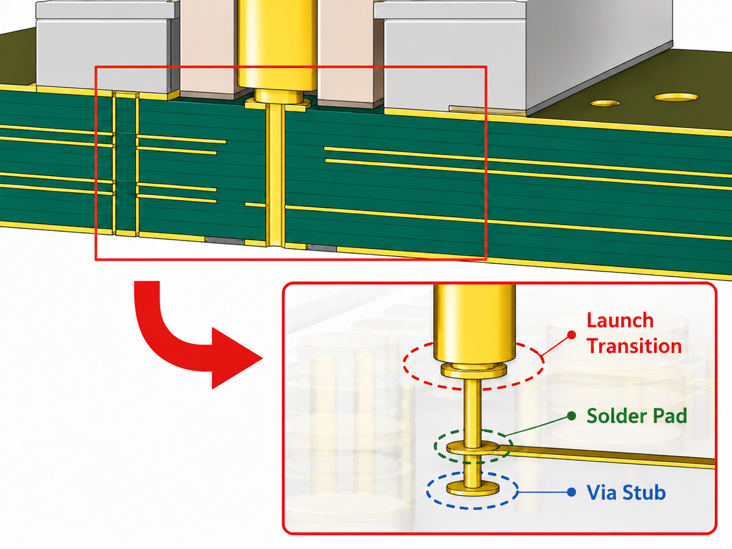
When a high-speed signal encounters an impedance discontinuity, a portion of the signal energy is reflected toward the source, degrading return-loss performance. Common discontinuities occur at connector-to-PCB launch transitions, pads, vias, trace bends, and changes in the grounding structure.
Fixture impedance must be designed according to the signal architecture of the product. Coaxial interconnects are typically designed around a 50 Ω single-ended characteristic impedance, while differential interconnects commonly use a 100 Ω differential impedance target.
During fixture development, HULANE analyzes and optimizes the connector launch region, pad geometry, via structures, and grounding configuration to provide a smooth transition from the connector into the fixture PCB and reduce reflections caused by impedance discontinuities.
2. Minimize Signal-Path Length to Reduce Insertion Loss
As frequency increases, conductor and dielectric losses also increase. High-frequency PCB loss is influenced by skin effect, dielectric properties, copper-foil roughness, trace length, and the number of transitions in the signal path.
High-frequency fixtures should therefore follow the principles of short paths, minimal transitions, and simplified structures. Unnecessary bends, vias, and interconnect transitions should be avoided wherever possible.
In addition to trace length, dielectric constant, dissipation factor, and material stability affect high-frequency transmission performance. During the initial design phase, the PCB material and stackup must be selected according to the target frequency range and product requirements so that fixture loss does not mask the performance of the DUT.
Coordinated optimization of routing, materials, and structure minimizes the fixture contribution to insertion loss, preserves the usable signal, and produces measurements that more closely represent the actual performance of the DUT.
3. Maintain Differential Symmetry to Reduce Crosstalk and Mode Conversion
High-speed interfaces such as HSD and Automotive Ethernet typically use differential signaling. Because data is transmitted over two conductors with opposite polarity, differential channels are highly sensitive to trace length, spacing, structural symmetry, and return-path continuity.
Length mismatch, excessive spacing variation, asymmetric transitions, or inconsistent grounding can introduce skew, differential imbalance, crosstalk, and mode conversion.
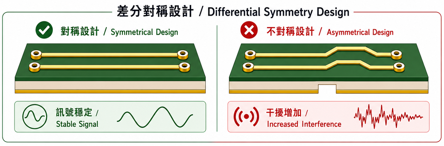
These effects not only degrade signal quality but can also prevent the measured data from accurately representing the differential performance of the product.
For differential test fixtures, HULANE places particular emphasis on pair-length matching, consistent pair spacing, symmetric launch transitions, and continuous return paths. Channel spacing and grounding structures are also optimized to reduce electromagnetic coupling between adjacent signals and support stable high-speed transmission.
Pre-Layout Planning: Reducing Risk at the Source
The performance of a high-frequency fixture is often determined before PCB routing begins.
Pre-layout planning verifies the PCB stackup, material system, transmission-line geometry, impedance targets, via structures, and grounding approach before detailed routing. This helps reduce the risk of impedance deviations, excessive loss, and inaccurate measurement data before detailed layout begins.
PCB Stackup and Material Selection
PCB materials have different dielectric constants and dissipation factors. As the test frequency increases, material properties have a greater impact on signal attenuation and phase stability.
During the initial fixture design phase, the laminate, copper thickness, and layer arrangement are selected based on the target frequency range, impedance requirements, and board-thickness constraints. Signal, ground, and power layers are then arranged to provide stable reference planes for the transmission lines.
.png)
Transmission-Line Structure Planning
Common transmission-line structures used in high-frequency PCBs include microstrip and stripline.
Microstrip routing is located on an outer PCB layer and provides convenient access to connectors and test ports, but it is more susceptible to external influences. Stripline routing is embedded between reference planes and provides better shielding, although the associated transitions and via structures are more complex.
The appropriate transmission-line structure is selected according to the product architecture, test-port location, and frequency requirements. Trace width, copper thickness, dielectric thickness, and reference-plane configuration are then designed to achieve the target impedance.
.png)
Via and Backdrill Design
When high-speed signals change PCB layers through vias, the unused portion of the plated through-hole can form a via stub. At higher frequencies, this parasitic structure may cause reflections and resonances.
High-frequency fixtures therefore require optimization of via diameter, pad and antipad geometry, and ground-via placement. Where necessary, backdrilling is used to remove unused via stubs and reduce the risk of resonance and reflection.
.png)
Comprehensive pre-layout planning confirms trace lengths, channel spacing, transition schemes, and electrical feasibility in advance. This improves fixture testability while reducing redesign and repeated-validation costs.
.png)
Post-Layout Validation: Confirming the Design Through Simulation
After PCB layout is complete, post-layout analysis is still required to confirm that the implemented design meets expectations.
High-frequency performance is sensitive to small geometric details. Even when the initial impedance calculations are correct, pads, vias, connector launch regions, reference-plane voids, and trace bends in the final layout can introduce additional parasitic capacitance and inductance.
HULANE therefore performs electrical simulation on the completed fixture layout to evaluate insertion loss, return loss, impedance continuity, channel crosstalk, and mode conversion.
Time-domain reflectometry (TDR) is used to observe impedance variation along the signal path and locate discontinuities. S-parameter analysis is used to evaluate insertion loss, return loss, and inter-channel coupling across frequency.
If simulation identifies an impedance discontinuity, excessive loss, or crosstalk risk, the engineering team can refine the routing, pad geometry, via structures, or grounding before fabrication, reducing the risk of discovering issues only after the physical fixture has been built.
.png)
Dual Validation Through Simulation and Measurement
Full-wave electromagnetic simulation enables engineers to predict the transmission behavior of the fixture, but simulation results must still be validated through physical measurement.
HULANE uses a dual-validation approach combining electromagnetic simulation and physical testing. After fabrication, the fixture is measured in HULANE’s in-house high-frequency laboratory using a vector network analyzer (VNA). The measured S-parameter data is then correlated with the simulated results.
Correlation between simulation and measurement helps confirm whether material properties, manufacturing tolerances, connector models, and fixture structures are consistent with the original design assumptions.
When differences are identified, engineers can investigate the source of error and refine the fixture model or physical design. This creates an iterative validation loop linking simulation, measurement, and product development.
This process not only confirms fixture performance but also provides reliable data for subsequent product optimization.
How Does De-Embedding Reveal the Intrinsic Performance of the DUT?
In an actual high-frequency measurement, the signal typically passes through test cables, adapters, launch transitions, the fixture PCB, and the DUT. As a result, the data measured by the VNA includes the combined response of the entire measurement system.
Using raw, uncorrected data may make it difficult to determine whether observed loss or reflection originates from the DUT or from the fixture, cable, adapters, and transitions.
De-embedding first characterizes the electrical response of the fixture and transition structures, then mathematically removes their contribution from the overall measurement. This shifts the reference planes to the DUT interfaces and reveals the intrinsic electrical characteristics of the DUT.
After de-embedding, engineers can more accurately evaluate insertion loss, return loss, impedance, and crosstalk performance.
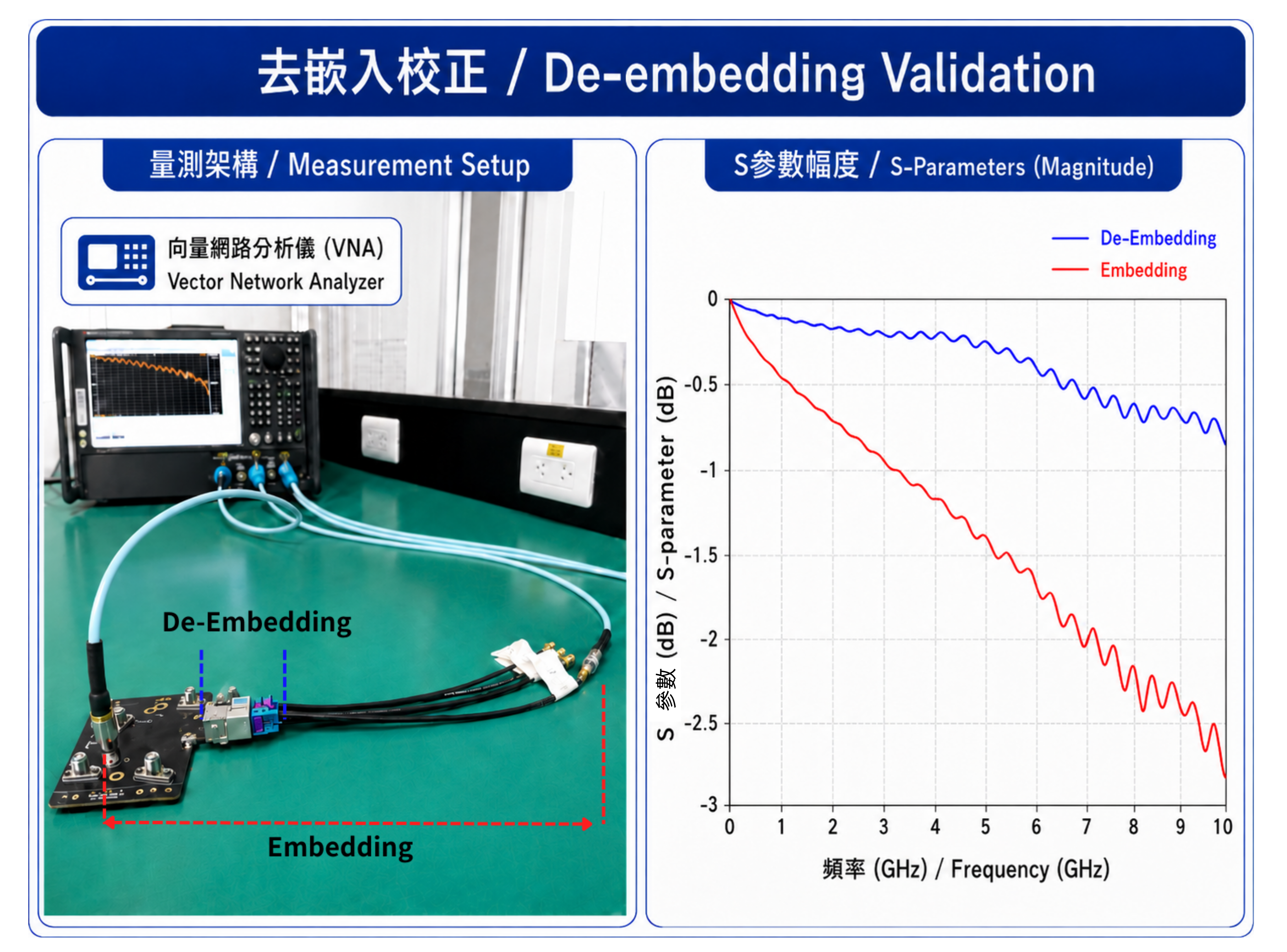
For high-frequency and high-speed connectors, de-embedding is not merely a post-processing step; it is a critical element of measurement integrity. Fixture design, electromagnetic simulation, physical measurement, calibration, and de-embedding must work together to ensure that the final data has sufficient accuracy and engineering value.
Key Test Fixture Design Considerations for FAKRA and Mini FAKRA
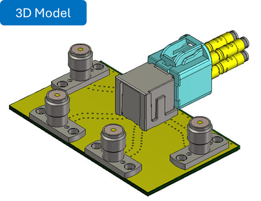
FAKRA and Mini FAKRA use coaxial signal architectures. The signal enters the connector through a coaxial cable and transitions from the connector into the PCB test fixture.
The key design objective for a coaxial fixture is to maintain a 50 Ω characteristic impedance and provide a smooth electrical transition between the coaxial structure and PCB transmission line.
Geometric discontinuities between the connector contact, pad, ground contacts, and PCB transmission line can create impedance steps and cause high-frequency reflections at the launch transition.
HULANE optimizes impedance matching, grounding structures, pad geometry, and the connector-to-PCB launch transition to reduce reflection and loss as the signal transitions from the coaxial interface into the PCB. This improves the repeatability and stability of RF measurements for FAKRA and Mini FAKRA products.
.png)
Key Test Fixture Design Considerations for HSD and Automotive Ethernet
Unlike coaxial interfaces, HSD and Automotive Ethernet use differential signaling and therefore require tighter control of balance and symmetry between the two signal conductors.
At high data rates, pair-length mismatch, spacing variation, asymmetric launch transitions, or inconsistent grounding can introduce skew, crosstalk, and mode conversion, affecting differential insertion loss, differential return loss, and common-mode performance.
During HSD and Automotive Ethernet fixture development, HULANE evaluates pair-length matching, channel spacing, grounding structures, launch symmetry, and signal return-path continuity as an integrated system.
Electromagnetic simulation and measurement validation are then used to characterize impedance, loss, and crosstalk across the target frequency range. By reducing fixture-induced disturbance to the differential channel, the resulting measurements more accurately represent the intrinsic high-speed transmission performance of the product.
.png)
Building Trusted High-Frequency Test Capabilities from Fixture Design Through Product Validation
A well-designed high-frequency test fixture enables measurement results that accurately represent the intrinsic electrical performance of the DUT.
For automotive high-frequency and high-speed connectors—including FAKRA, Mini FAKRA, HSD, and Automotive Ethernet—HULANE integrates test fixture design, PCB layout analysis, electromagnetic simulation, signal integrity validation, physical measurement, and de-embedding into a unified development process.
Supported by an in-house high-frequency laboratory and vector network analyzer capability, HULANE correlates simulated and measured data to evaluate the electrical performance of both the product and the test fixture while minimizing the influence of fixtures, transitions, and the measurement system.
This closed-loop validation process improves measurement accuracy, repeatability, and confidence. It also enables the engineering team to identify design risks earlier and provides reliable data for subsequent performance tuning, structural optimization, and product validation.
Through in-house capabilities spanning design, simulation, and physical measurement, HULANE continues to strengthen the development foundation for automotive high-frequency connectors and address the growing demand for high-speed, stable, and reliable in-vehicle data transmission.